The field of photonics, the science of controlling and manipulating light at the nanometer scale, is on the verge of a structural paradigm shift. Traditionally, the design of photonic devices—such as metasurfaces and subwavelength structures—has relied on laborious trial-and-error processes or computationally expensive simulations. However, a new research approach utilizing diffusion models, the same technology powering generative AIs like DALL-E and Midjourney, promises to revolutionize the status quo.
Recent research highlighted by Newswise details how Artificial Intelligence can now 'generate' physical structures based on desired optical properties. Instead of a scientist designing a structure and testing its performance (forward design), the AI model accepts the desired outcome as input—for instance, a specific light refraction or absorption pattern—and automatically generates the geometric shape to achieve it. This process, known as inverse design, is now attaining unprecedented speed and precision.
From Pixels to Physics: How Diffusion Models Work
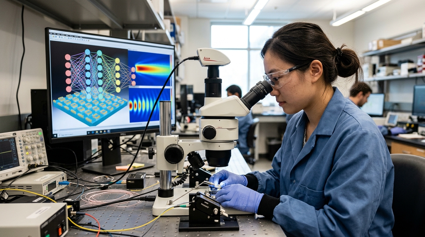
Diffusion models function by learning to reverse a noise-addition process. In image generation, the model starts with 'white noise' and gradually refines it until a clear image emerges. In the context of photonics, the 'noise' does not represent pixels, but the geometric parameters of a subwavelength structure. The model is trained on vast datasets that link physical shapes with their corresponding optical responses.
The breakthrough aspect of this study is the model's ability to directly map optical properties to structures that are smaller than the wavelength of light. These structures, which often resemble complex, maze-like patterns, are nearly impossible to design using human intuition alone. AI can explore a design space of billions of possibilities within seconds, identifying solutions that traditional optimization algorithms would take days to approach.
Applications: From Telecommunications to Medical Imaging
The implications of this technology span multiple industries. In telecommunications, designing more efficient photonic circuits can lead to faster data transfer with minimal energy consumption. As we approach the limits of Moore's Law for electronic chips, photonics offers a viable path forward, using photons instead of electrons.
- Metalenses: Replacing bulky glass lenses with flat surfaces nanometers thick, which can be utilized in smartphones and medical endoscopes.
- High-Sensitivity Sensors: Creating structures that trap light in ways that allow for the detection of single molecules, crucial for early disease diagnosis.
- Quantum Computing: Designing the photon sources and gates necessary for the operation of large-scale quantum systems.
Furthermore, the use of diffusion models allows for the creation of structures that are resilient to manufacturing defects. At the nanoscale, even the slightest deviation can ruin a device's performance. AI can be trained to suggest designs that maintain their properties even if the manufacturing process is imperfect, thereby reducing production costs.
The Interpretability Challenge and the Path Ahead
Despite the excitement, the use of generative AI in physics raises questions. Scientists often refer to these models as 'black boxes.' While the AI can find the ideal structure, it doesn't always explain *why* that structure works the way it does from a physical standpoint. The challenge for the coming years will be bridging the gap between computational power and theoretical understanding.
"We are not just building better tools; we are changing the way we perceive the relationship between geometry and light," the research team notes.
In conclusion, the integration of diffusion models into photonics marks a new era of 'intelligent materials.' The ability to define a desired function and let AI realize its physical form is a power that will accelerate innovation at rates traditional science could never have imagined. The future of technology is now literally written in light, designed by the machine.